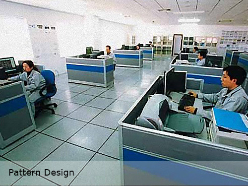
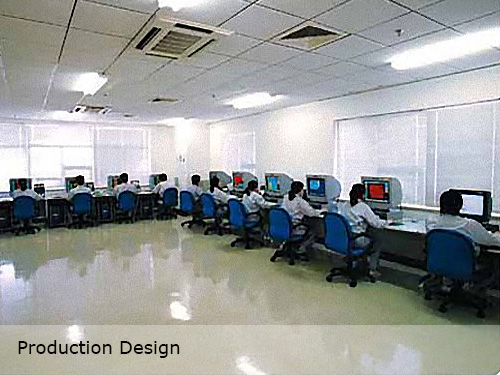
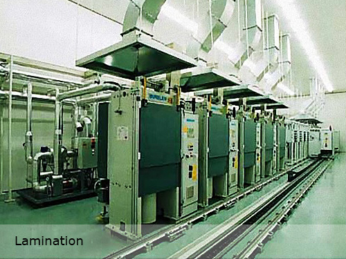
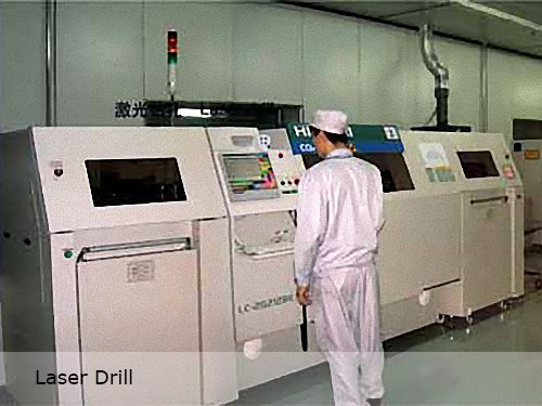
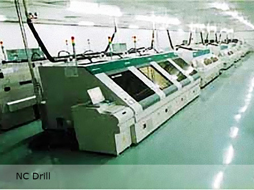
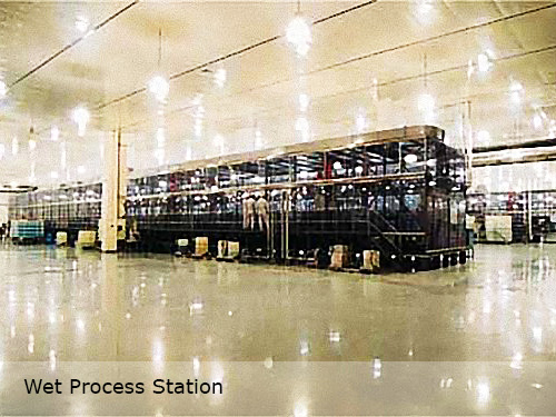
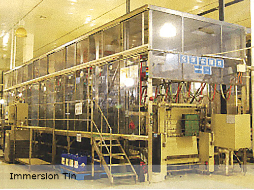
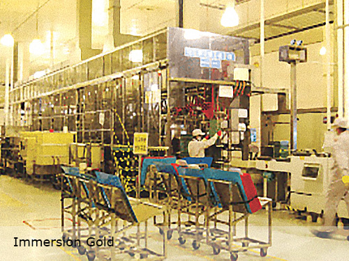
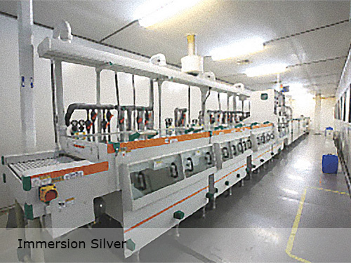
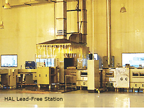
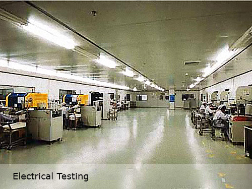
Our China manufactoring facilities are among the best in the PCB industry with over 25 years of experience. Each location has obtain ISO9001, ISO14001, ISO/TS16949, UL certified and RoHS certified.
In addition of manufacturing traditional rigid PCBs, we have experience of producing cutting-edge electronic products using the High-Density Interconnect (HDI) , IC packaging and other high-tech system to provide a broad space for development in the field of printed circuit boards.
The products are widely applied in different fields, such as industrial automation control, telecommunication, mobile phones, aviation and aerospace, automotive electronics, IT, instrument and meters, medical devices and consumer electronics.
- Double-sided ~ High Multi-layer PCB (max. 40-layer)
- HDI (2+X+2 Build UP)
- HDI thin PCB (0.25mm for 4-layer, 0.40mm for 6-layer)
- Big size, Back plane PCB (Panel size at 24”x36”, Thickness of 4.5mm or more)
- Special-purpose PCB (Heavy copper(6oz) PCB, / Buried resistance PCB)
- Via hole copper plating
- Thick gold
- Uneven gold finger
